Orthogonal Update – Solutions for Organic Photodetectors for Under the Display Fingerprint Sensors Expected to Be Commercialized in 2020
GeneralOne of the leading companies developing OLEDs patterned by photolithography instead of fine metal masks (FMMs) is a US start-up called Orthogonal. Printed Electronics Now recently did a story on them and I thought it was worth including some of the highlights. In addition, I interviewed two of their executives, founder, EVP and CTO Dr. John DeFranco and Victor Hsia, VP of Business Development, to get more insight into their status, plans and outlook.
Orthogonal was founded as a Cornell University spin-out based on research by Dr. John DeFranco and his collaborators. With the goal of utilizing photolithography rather than FMMs, Orthogonal has attempted to developed resist solutions which would allow the same line to make TVs as well as mobile displays. Since photolithography is on the frontplane, it can also boost resolution of the display to 2000 PPI or higher. In addition to OLEDs, their resist solutions can also be used for organic photodetectors which could allow an under-the-dis- play fingerprint sensor as large as the display and also allow multiple fingers to be used at the same time. According to DeFranco who is now EVP and CTO, “The fundamental invention was photoresist chem- istry (based on fluorinated solvents) that allowed direct patterning of chemically sensitive materials, particularly organic electronics, using photolithography.”
The company was spun out in 2009, received initial grant money from the National Science Foundation SBIR program and established a lab in Ithaca, NY.
According to DeFranco, “Early interest in the technology came from some large Taiwanese display companies that were working on organic thin film transistors (OTFT) for flexible e-paper backplanes.” This was likely CPT as it has collaborated with others in this area.
DeFranco went on to say “Orthogonal signed an early joint development agreement with AZ Electronic Materials to develop the technology for the OTFT market. After the iPad was released, this market slowed significantly and we were forced to pivot towards OLED around 2014. It was starting to be clear that the existing paradigm for manufacturing, fine metal mask (FMM), was severely limited, as evidenced by Samsung abandoning the OLED TV market due to manufacturing issues.”
Orthogonal continues to develop its OLED solution which is making progress. Although I have not seen a prototype, apparently there is a 3-color passive matrix OLED prototype and Dr. DeFranco will have it at SID. He indicated they are still bringing in equipment which should result in more advanced prototypes and allow them to demonstrate the lifetime of their material. Their technology could enable very high resolution displays for the AR/VR industry, improve battery life in the mobile market as well as enable directly patterning OLEDs for TVs, representing a complete solution for OLED display manufacturing across the maximum range of panel sizes. It would also boost demand for photolithography, coater/developer and dry etch equipment.
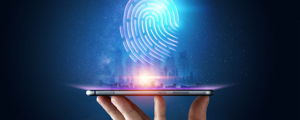
While there is an opportunity in displays, there is a nearer term commercial opportunity for their materials in organic photodetectors for fingerprint sensing. Today’s fingerprint sensors are primarily built using CMOS capacitive technology and are built on silicon chips as large as a fingerprint. Organic photodetectors are a positive for display manufacturers as they could be produced by the display supplier, boosting their value in the smartphone supply chain. They could be produced on glass, carrier glass, roll to roll on plastic, screen printed on PET, etc. For this application, resolution is very high, around 500PPI, so it would likely be produced on glass or carrier glass, which represents another market opportunity for Corning. Only for foldable displays would it need to be flexible today, although certainly it would be lighter if lifted off the glass. It is also a win for smartphone brands as having a larger fingerprint sensor which could allow for multiple fingers should be popular with consumers.
In addition to allowing a larger fingerprint sensor, organic photodetectors are believed to be 5-10X more sensitive than CMOS sensors at the wavelengths used which are around infrared. For example, there have been some concerns that the Qualcomm Ultrasonic solution doesn’t work with screen protectors. The organic photodetectors work by converting incident light or photons into information. A high EQE or conversion ratio of incident photons to current is obtained by blending two organic semiconductors, a p-type and n-type, sandwiched between two electrodes. Excitons generated by photons are separated into electrons and holes to create current that can be measured for signal processing.
One of the challenges with the organic materials is that there needs to be a way to pattern them to achieve 500 PPI while ensuring they don’t fail. Like OLEDs, the organic materials in photodetectors are also vulnerable to moisture, oxygen, water and can have short lifetimes. This is where Orthogonal steps in. Their fluorine based photoresist chemistry can protect these materials and allow them to be patterned at desired resolutions.
Another challenge for organic photodetectors will be costs. Synaptics, Goodix Technology and others have been ramping, have achieved high volumes and are driving down the costs. However, the opportunity for the panel supplier to take this on, the greater sensitivity at infrared as well as the larger size of the fingerprint sensor gives organic photodetectors a real chance to take significant share.
According to DeFranco, the leading suppliers of the organic materials used in photodetectors are Sumitomo Chemical and Merck. Their new CEO, David Fyfe, is very familiar with these companies. Fyfe was chair- man and CEO of Cambridge Display Technology from 2000 to 2010. Fyfe took the company from an R&D shop to a Nasdaq listing in 2004 and a sale to Sumitomo in 2007 for $285M. Fyfe told Printed Electronic Now that “Customers are initially skeptical of a solvent system that does not damage organic materials. The principle proof point Orthogonal needs to show to customers is a robust set of performance measurements of organic devices processed with Orthogonal chemicals. With a recently acquired tool, this is greatly accelerated. We expect commercialization of photoresist for the fingerprint sensing market by late 2020, with the OLED market taking shape soon thereafter.”
I also asked DeFranco about their business model. He indicated that although they have established significant IP in fluorinated photoresists and solvents, their business model will be based on material sales and they will work with a large materials supplier to produce their materials. When asked which panel supplier is likely to be first in implementing their technology, he indicated it will likely come from China.