Orthogonal Merges OLED Materials and Photolithography
GeneralKey opportunities include organic photodetectors for fingerprint sensing, VR and TV displays.
David Savastano, Editor 04.17.19
There is plenty of development occurring in the display field, with OLEDs being an area where printing is seen as a strong possibility. Already, companies like JOLED are printing smaller displays. One key is to develop materials that allow OLED manufacturers to print their displays.
Orthogonal is one of the leaders in the field of OLED materials. Orthogonal was founded as a Cornell University spin-out based on research by Dr. John DeFranco and his collaborators. With an eye on utilizing photolithography, Orthogonal’s photoresist solutions allow direct patterning of a wide range of organic electronic materials. These materials can be used for high-resolution OLED displays and flexible display applications as well as organic sensors for the virtual reality, mobile and television markets.
“The fundamental invention was photoresist chemistry (based on fluorinated solvents) that allowed direct patterning of chemically sensitive materials, particularly organic electronics, using photolithography,” said Dr. DeFranco, Orthogonal’s co-founder as well as its EVP and CTO.
Dr. DeFranco decided that the commercial applications for this technology were numerous, and he spun out the company in 2009. The company received initial grant money from the National Science Foundation SBIR program and established a lab in Ithaca, NY.
“Early interest in the technology came from some large Taiwanese display companies that were working on organic thin film transistors (OTFT) for flexible e-paper backplanes,” Dr. DeFranco noted. “Orthogonal signed an early joint development agreement with AZ Electronic Materials to develop the technology for the OTFT market. After the iPad was released, this market slowed significantly and we were forced to pivot towards OLED around 2014.”
At the time, the OLED market was starting to grow rapidly, but Dr. DeFranco noted that it was also changing rapidly.
“It was starting to be clear that the existing paradigm for manufacturing, fine metal mask (FMM), was severely limited, as evidenced by Samsung abandoning the OLED TV market due to manufacturing issues,” he observed. “Orthogonal continued to develop its OLED solution, which is today close to commercial projects.
More recently, another more near-term commercial opportunity appeared in the area of organic photodetectors for fingerprint sensing applications, and Orthogonal is now developing that technology alongside its OLED solution.
Dr. DeFranco noted that Orthogonal’s materials enable industry-standard photolithography to be used in the patterning of organic electronic materials.
“Photolithography is a mature technology that is widely used in the display and semiconductor industries and is capable of high resolution and large area patterning,” he said., “For OLED, this means the precise placement of pixels, large or small across a large area, all done on existing manufacturing equipment. It enables ultra-high resolution displays for the VR/AR industry, dramatically increases the fill factor (increasing display lifetime) for mobile phone applications and enables directly patterned OLED for TV applications.
“Orthogonal’s technology is the only one with the promise of enabling high resolution and large area patterning using existing mature equipment, without significantly degrading the devices,” Dr. DeFranco added. “It would represent a complete solution to OLED display manufacturing.”
Recently, Orthogonal added to its leadership team by bringing in David Fyfe to serve as CEO. Long active in the OLED field, Fyfe served as chairman and CEO of Cambridge Display Technology Limited (CDT) from 2000 to 2010. Under his leadership, CDT went from a lab-based venture to a Nasdaq flotation in 2004 and a sale to Sumitomo Chemical for $285 million in 2007.
“David is a real heavyweight in the OLED industry, and we are truly excited to be under his leadership,” said Dr. DeFranco. “He brings a breadth of knowledge and skillset from over 30 years as CEO to enable Orthogonal to move to the next level.”
Fyfe said that many potential customers are excited by the prospect of patterning using photolithography and eliminating FMM.
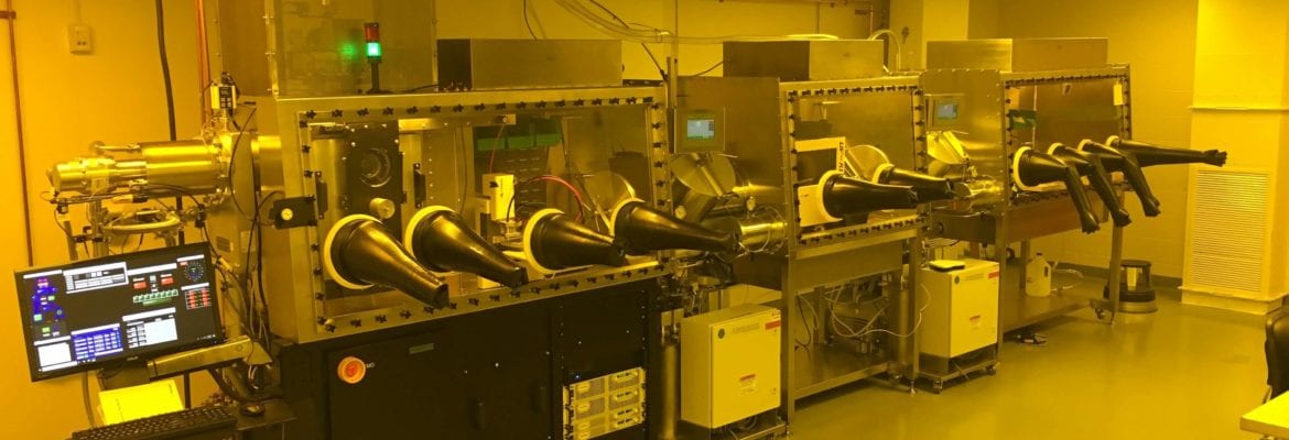
“They are skeptical of a solvent system that does not damage OLED materials,” added Fyfe. “The principle proof point Orthogonal needs to show to customers is a robust set of performance measurements of OLED devices processed with Orthogonal chemicals. With a recently acquired tool, this is greatly accelerated.”
Fyfe said that he anticipates Orthogonal’s products reaching the market in the next year.
“We expect commercialization of photoresist for the fingerprint sensing market by late 2020, with the OLED market taking shape soon thereafter.”
Originally posted: https://www.printedelectronicsnow.com/contents/view_online-exclusives/2019-04-17/orthogonal-merges-oled-materials-and-photolithography/